
Nvidia's A16 Conundrum: Market Speculation vs. Analyst Skepticism on Process Node Strategy & Supply Chain Diversification
Will Nvidia break its long-standing "n-1" process node strategy to embrace TSMC's cutting-edge, yet costly, A16 for its next-gen AI accelerators, or is there more to the story than market whispers suggest, pointing to a diversified and nuanced approach to high-performance computing?


Market Rumors and Analyst Views: The Dynamics of Nvidia and TSMC's A16 Process Node Adoption
Recent market rumors suggest that Nvidia is poised to be an early adopter of TSMC's A16 process node, aiming for significant performance gains through backside power delivery technology. While this move could entail substantial costs, Nvidia, with its high Average Selling Prices (ASPs) for AI accelerators, appears to have a strong economic incentive to "pay for value." However, analysts from BNP Paribas London Branch maintain a cautious stance on these rumors, suggesting a potential conflict with Nvidia's publicly announced GPU roadmap and its long-standing "n-1" process node strategy for GPUs.
TSMC's A16 Process Node: A Pivotal Shift and Technological Breakthrough in the AI Era
TSMC's A16 process node is anticipated to enter mass production in the second half of 2026, marking a significant milestone where AI applications will, for the first time, drive the adoption of TSMC's most advanced manufacturing technology. The core innovation of the A16 process lies in the introduction of backside power (SPR) technology, which is considered crucial for enhancing chip performance and density.
Historically, advanced semiconductor manufacturing was primarily driven by the smartphone market. However, in recent years, with the explosion of AI demand, AI applications are progressively displacing smartphones as the primary force propelling the development of advanced semiconductor processes. For instance, AMD also plans to launch its 2nm process node-based HPC (High-Performance Computing) chip, the Venice CPU, in 2025.
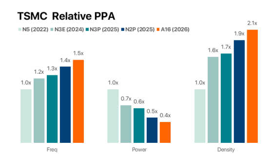
The inaugural introduction of backside power (SPR) technology in the A16 process node is expected to deliver significant power efficiency and performance improvements for HPC logic devices. Compared to Nvidia's current N5-based GPUs, A16 can offer a 1.5x performance boost or reduce power consumption by 60% at the same voltage.
A16 Process Performance Improvement vs. Nvidia N5 GPU Comparison
Source: BNP
Speculation of Nvidia's Early A16 Adoption and its Economic Drivers
Sources from the Taiwanese supply chain indicate that Nvidia could become one of the first customers for TSMC's A16 process node in the second half of 2026, intending to integrate this technology into its future Feynman architecture. This would mark Nvidia's return to utilizing TSMC's most advanced process technology since the 0.11-micron node.
The 'Paying for Value' Rationale Amidst High Costs: Despite the high costs associated with advanced processes, customers remain willing to pay a premium for technologies like A16. For example, a 2nm wafer costs nearly $27,000, while the backside power delivery version of the A16 process node, which Nvidia reportedly plans to adopt, is expected to be even more expensive, exceeding $30,000 per wafer.
The economic impetus for Nvidia's shift towards the most advanced processes lies in the high ASPs of its AI accelerators. It is estimated that by the end of 2026, the cost per chip for both N3P and A16 nodes, at the same defect density, would increase by approximately $300-400. For a Rubin Ultra GPU comprising 4 chips, this translates to an approximate $1,200 increase in chip cost. To maintain an 80% gross margin, this could result in a final product price increase of approximately $6,000. However, in the high-demand and supply-constrained AI accelerator market, where ASPs already exceed $60,000, such cost increases can be passed on to customers, enabling Nvidia to absorb the higher process costs.
Analysts' Prudent Stance: Conflicts with Nvidia's GPU Roadmap and Conventional Wisdom
BNP Paribas London Branch analysts Jakob Bluestone and Kohulan Paramaguru express skepticism regarding rumors of Nvidia adopting the A16 process node, positing that Nvidia will likely adhere to its "n-1" process strategy. Their primary rationale stems from conflicts between Nvidia's previously announced GPU roadmap and the launch timeline and node nomenclature of A16.
Nvidia's recent public roadmap indicates:
- Second half of 2025: Blackwell Ultra (N5)
- Second half of 2026: Rubin (N3)
- First half of 2027: Rubin Ultra (N3)
- Second half of 2027: Feynman (N2)
If Nvidia were to become the first customer for A16 by the end of 2026, it would imply that either Rubin or Rubin Ultra might utilize A16. However, both Rubin and Rubin Ultra were designated as N3 GPUs in 2024, which conflicts with the A16 node's nomenclature (categorized as an N2-class node). Furthermore, Nvidia has not adopted the most advanced process node for over 15 years.
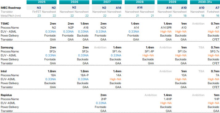
TSMC Advanced Process Roadmap
Source: BNP
NVIDIA Data Center GPU/CPU Product Roadmap (2024 - 2027) Nvidia plans to introduce new data center GPU products annually, continuously advancing HBM memory stack upgrades. In 2024, the Blackwell GPU will be launched, paired with HBM3e 8-high memory. 2025 will see the introduction of the Blackwell Ultra GPU, with memory upgraded to HBM3e 12-high. In 2026, the Rubin GPU will be launched, marking the debut of the Vera (ARM) CPU, with memory upgraded to HBM4. 2027 will feature the Rubin Ultra GPU, continuing with the Vera CPU and HBM4 memory. This roadmap clearly indicates that the Rubin series GPUs will utilize HBM4 memory and operate in conjunction with the Vera (ARM) CPU, presenting inconsistencies with the A16 process node rumors in terms of both timeline and process node.
Nvidia's Diversified High-Performance Computing Strategy: CPUs, CPX, and Interconnect Technologies
Beyond considerations for GPU process nodes, Nvidia is also focusing on multiple fronts to enhance the performance and integration of its server solutions.
Arm Architecture CPU Strategy: Nvidia designed the Grace CPU, its first Arm-based CPU, for the Grace Hopper and Grace Blackwell superchips. In the future, Nvidia plans to launch the Vera (ARM) CPU concurrently with the Rubin GPU in 2026, replacing the Grace CPU. The Arm architecture offers advantages in the server domain, including lower costs and reduced power consumption, leading many large hyperscalers to adopt it. Nvidia is also actively expanding into the Arm PC market, collaborating with MediaTek to develop the Arm-based PC chip, NVIDIA N1X, expected for release in 2025. Currently, Nvidia's GB10 chip, which combines the Blackwell GPU and Grace CPU, has entered mass production at TSMC and is expected to ship in volume as early as the second half of 2025.
NVIDIA Rubin CPX: This is a new category of GPU specifically designed for large-scale context processing. It enables AI systems to process millions of tokens for software coding and generative video applications with breakthrough speed and efficiency, featuring over 30 petaflops of NVFP4 computing power and CUDA support. The Rubin CPX incorporates new attention acceleration cores, making it 3x faster than the existing GB300 GPU. Jensen Huang stated that the Rubin CPX is the first CUDA GPU specifically engineered for large-scale context AI.
Also see:
 Jason & Jarvis
Nvidia's Interconnect Technology (NVLink) and Chiplet Strategy: NVLink is a core advantage for Nvidia in network connectivity, enabling "horizontal scaling" (scale-up) where multiple chips operate as a single large chip. Through its NVLink Fusion strategy, Nvidia licenses its chip-to-chip (C2C) technology and sells NVLink Fusion chiplets. By designing "superchips" that directly integrate Grace CPUs with the latest GPUs on the same silicon, Nvidia achieves an order-of-magnitude faster connection, exemplified by Grace Hopper and Grace Blackwell.
Potential Collaboration with Intel's 14A Process: Rumors suggest that Nvidia is considering adopting Intel's 14A process node for its future chips. This could be a potential breakthrough for Intel Foundry's business, helping to challenge TSMC's dominant position in the wafer foundry sector. Nvidia might first employ the 14A process for its lower-end Game GPUs, products targeting the entry-level market with approximately 2,000 cores and power consumption not exceeding 200 watts. Collaborating with Intel could allow Nvidia to mitigate its reliance on TSMC and expand its product matrix, covering a broader range of price points. Intel's 14A process is projected to enter mass production after 2027, offering technological advantages such as PowerVia, second-generation RibbonFET transistors, and PowerDirect technology.
Profound Impact of Advanced Process Nodes on the Semiconductor Supply Chain
If the rumors of Nvidia adopting A16 prove true, it would positively impact the leading edge WFE (Wafer Fab Equipment) market, particularly benefiting wafer manufacturing equipment suppliers like ASML and ASM. Nvidia's entry would intensify competition among companies like Apple, AMD, Intel, and Qualcomm for the most advanced wafer capacity. This could accelerate the ramp-up of future nodes such as A14 and A10. Current projections estimate TSMC's N2-class nodes (including A16) to reach a design capacity of 100,000 wafers by the end of 2026 and 150,000 wafers by the end of 2027. TSMC's A16 process node is anticipated to launch by the end of 2026; the N2P process node is expected to enter production by the end of 2025.
Competitive Landscape and Future Outlook
Despite skepticism surrounding Nvidia's potential adoption of A16, logically, the additional advantages offered by A16 (e.g., a 40% reduction in power consumption compared to N3P) would further widen Nvidia's performance gap over competitors. Through comprehensive system design, Nvidia is expected to maintain an AI accelerator market share exceeding 80%. However, moving to the bleeding-edge process node also represents certain risks. Concurrently, Nvidia faces challenges such as market competition and data center power consumption limitations. Its diversified high-performance computing strategy, encompassing CPUs, CPX, and interconnect technologies, collectively forms its competitive moat in the AI era.


