
Nvidia Acquires Enfabrica to Tackle AI's Memory Wall with Converged Interconnects
Nvidia is the undisputed king of AI chips, so why did it just spend nearly a billion dollars not on another chipmaker, but on a little-known interconnect startup?


Nvidia's Strategic Gambit: A $900 Million Acquisition of Enfabrica to Tackle AI's "Memory Wall"
Recently, a seemingly low-key deal sent ripples through the tech investment community: AI chip giant Nvidia acquired the AI networking startup Enfabrica, along with its star CEO Rochan Sankar and core team, for over $900 million in cash and stock through an "acqui-hire."
This wasn't a traditional corporate merger but rather a precision strike for talent and technology. In today's escalating AI arms race, why would Nvidia bet heavily on a company focused on "connection" rather than "computation"? The answer points to the most daunting and critical bottleneck in current AI development: memory. This transaction not only reveals Nvidia's strategic foresight but also paints a blueprint for the evolution of next-generation AI data centers.
The Urgent Crisis: The Coming "KV Cache Apocalypse"
To grasp the strategic significance of this acquisition, we must first understand a technical challenge that gives all AI giants a headache: the Memory Wall.
With the explosion of generative AI, particularly Large Language Models (LLMs), AI applications are evolving from simple Q&A to more complex, "Agentic AI" systems capable of long-context understanding, multi-turn conversation memory, and even multi-agent collaboration. This shift has led to an exponential increase in demand for computing power, but a more hidden crisis has emerged: memory capacity and bandwidth are becoming scarcer resources than compute cores.
The heart of the problem lies in a mechanism called the "Key-Value Cache" (KV Cache). During LLM inference (content generation), the model stores the attention states of previously processed text sequences in the KV Cache to avoid redundant calculations. This dramatically improves generation speed, especially for multi-turn conversations. However, the size of the KV Cache is directly proportional to factors like context length and batch size.
Just how terrifying are these numbers? Manoj Sukumaran, Chief Analyst at Omdia, provides a stunning estimate: for a mainstream model like Llama-3 70B serving 100 concurrent users, the required KV Cache size could be as high as 16 TB! This far exceeds the capacity of the extremely expensive High-Bandwidth Memory (HBM) found on today's top-tier GPUs like the H100/H200, which typically ranges from 80 GB to 141 GB.
When the KV Cache exceeds HBM capacity, the GPU is forced to "offload" parts of the cache to much slower host DRAM or even SSDs, or to recompute it when needed. Either way, this leads to a drastic drop in performance. The Time to First Token (TTFT) can skyrocket from milliseconds to seconds, severely degrading the user experience. Expensive GPU cores are left idle, waiting for data, causing massive resource waste and soaring costs.
This is what the industry calls the "KV Cache Apocalypse"—a fundamental bottleneck that threatens to choke the large-scale deployment of AI.
Paradigm Shift: From "Tightly-Coupled" to "Disaggregated Architecture"
Facing this towering "Memory Wall," the entire industry has begun to pursue a profound architectural revolution, centered on the idea of a "Disaggregated Architecture."
In traditional data centers, compute (CPU/GPU) and memory (DRAM/HBM) are tightly bundled within the same server. A disaggregated architecture, however, breaks down resources like compute, memory, and storage into independent, freely scalable pools connected by an ultra-high-speed interconnect (Fabric). This allows AI tasks to elastically allocate resources as needed. For example, a compute-intensive task can be assigned more GPUs, while a memory-intensive task can access a massive pool of memory, thereby maximizing resource utilization.
Mooncake Architecture Diagram
This diagram of Moonshot AI's Mooncake platform visually demonstrates the disaggregated concept in software: separating the compute-intensive Prefill stage and the memory-intensive Decoding stage into different clusters, and building a distributed KV Cache pool that spans across nodes.
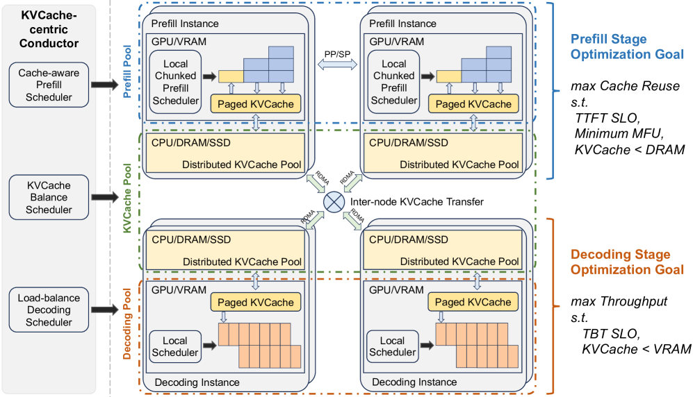
Under this new paradigm, innovation is happening on both the software and hardware fronts. Software solutions like Moonshot AI's Mooncake platform and LMSYS Org's SGLang HiCache optimize resource scheduling by building distributed caching systems centered around the KV Cache. But software optimizations have their limits. To fundamentally break down physical barriers, disruptive hardware innovation is essential.
And this is precisely where Enfabrica enters the stage.
Enfabrica's Ace in the Hole: Reshaping the AI Data Center Superhighway
Founded in 2019, Enfabrica has had an ambitious goal from the start: to fundamentally solve the interconnect bottleneck in AI data centers. Its core product is the "killer app" that caught Nvidia's eye.
1. The ACF-S SuperNIC: An All-in-One "Swiss Army Knife" for Switching and Networking
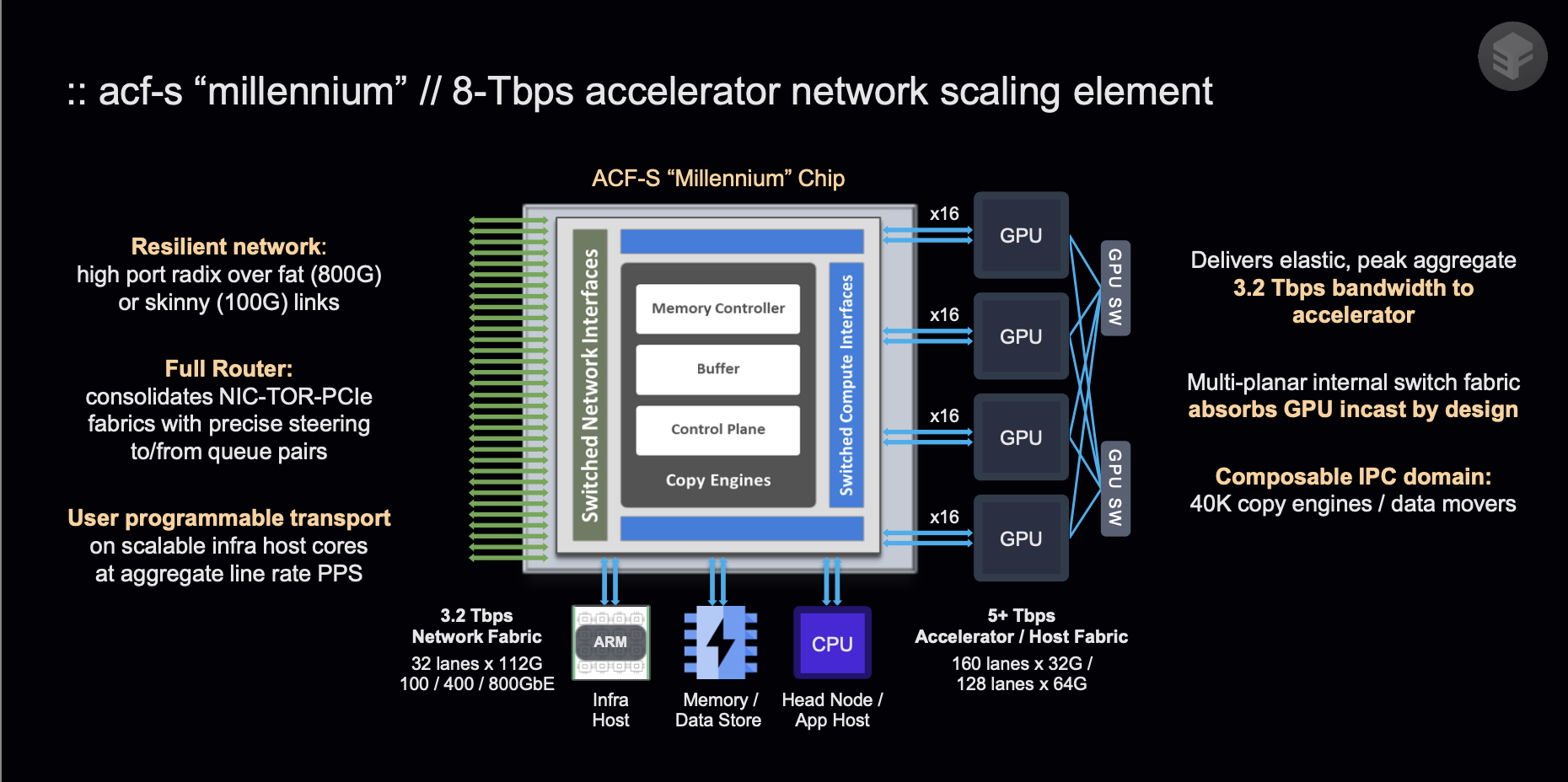
Enfabrica's foundational technology is its ACF-S "Millennium" chip, an incredibly powerful "SuperNIC" (Super Network Interface Card). On a single 5nm chip, it unprecedentedly fuses an Ethernet Packet Switch with a PCIe/CXL Memory Switch.
Enfabrica ACF-S "Millennium" Chip Architecture Diagram
Source: Enfabrica
Simply put, a traditional AI server requires a separate NIC for external communication and a separate PCIe switch to connect the CPU and GPUs. The ACF-S chip, however, plays multiple roles. It not only provides an ultra-high network bandwidth of up to 3.2 Tbps but also directly manages and schedules the GPUs, CPUs, and CXL memory devices connected to it. This vastly simplifies server design and eliminates internal data transfer bottlenecks.
2. EMFASYS: The "Infinite Memory Pool" for GPUs
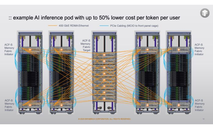
Building on the ACF-S chip, Enfabrica introduced its flagship solution: EMFASYS (Elastic Memory Fabric System). This system cleverly combines two key technologies, RDMA over Ethernet and CXL, to create a rack-scale shared memory pool accessible via standard Ethernet.
Enfabrica EMFASYS AI Inference System Diagram
Source: Enfabrica
The diagram above vividly illustrates how EMFASYS works: multiple GPU server racks can, via a high-speed network, collectively access a massive "memory pool" composed of inexpensive DDR5 DRAM. This pool can be used to offload enormous KV Caches, liberating the GPU's precious HBM for what it does best: computation.
According to Enfabrica's data, the EMFASYS system can expand an AI cluster's memory capacity by up to 18 TB, with a read latency of just 6 microseconds (100 times faster than SSDs), and can reduce the cost per token generated by up to 50%. For agentic AI applications that need to process ultra-long contexts, this is an undeniable game-changer.
Nvidia's Deeper Meaning: Acquiring the "Optimal Solution" to Complete the Strategic Puzzle
At this point, you might ask: Isn't Nvidia itself a networking giant? It acquired Mellanox in 2019 for a staggering $6.9 billion, and its InfiniBand technology is already the standard for AI clusters. Nvidia also recently announced its ConnectX-8 SuperNIC, which integrates PCIe switching. Why bother acquiring Enfabrica?
The answer is that Enfabrica's technology is likely superior to Nvidia's existing solutions in several key dimensions.
Comparison of Traditional Server Design and Optimized Design with ConnectX-8
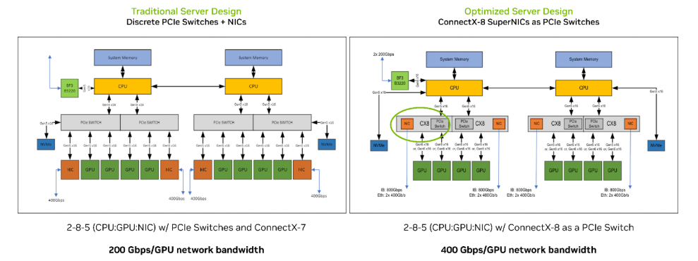
Nvidia's ConnectX-8 (right side of the image) does indeed simplify server design by integrating a PCIe switch, boosting network bandwidth per GPU to 400 Gb/s. This is a huge step forward.
However, technical analysis suggests that Enfabrica's ACF-S goes even further in its level of integration. It combines not just PCIe switching but also Ethernet switching, achieving a true "three-in-one" design. More critically, the ACF-S can offload tasks like cross-node communication and intra-node data forwarding entirely in hardware, consuming almost none of the GPU's precious compute resources (SMs). In contrast, Nvidia's current architecture still requires some GPU compute power for certain complex routing tasks.
In an era where "compute is power," any technology that can offload tasks from the GPU and increase its effective computational efficiency holds invaluable strategic value. What Nvidia saw was the superiority and immense potential of Enfabrica's architecture.
Therefore, this "acqui-hire" of over $900 million is, in essence:
- Acquiring Technology and Talent: Directly integrating the Enfabrica team and their leading converged interconnect architecture into the CUDA ecosystem to quickly shore up its own weaknesses in memory disaggregation.
- A Defensive Move: Preventing competitors (like AMD, Intel, or cloud giants with their custom ASICs) from obtaining this critical technology, thereby strengthening its own moat.
- Bypassing Scrutiny: Using an "acqui-hire" instead of a direct merger to cleverly circumvent increasingly strict antitrust reviews and achieve rapid integration.
Conclusion: Victory Belongs to the Master of Interconnectivity
Nvidia's acquisition of Enfabrica sends a clear signal: in the post-Moore's Law era, the focus of competition in AI infrastructure is shifting from a pure contest of chip performance to a higher-dimensional battle of system-level interconnectivity and resource orchestration.
The "Memory Wall" is the next great mountain that all AI players must climb. By bringing this crucial piece of the puzzle into its fold, Nvidia is not only paving the way for its own Grace Blackwell and Rubin platforms but is also declaring that the future hegemon of AI must not only build the fastest "engines" (GPUs) but also construct the widest and most intelligent "superhighway" (Memory Fabric) to connect them all.
This silent war over data center architecture has just begun. And Enfabrica is a key, strategic piece that Nvidia has placed on the board early in the game.


