
SK Hynix's First "Production Ready" High NA EUV Installation - Strategic Testing for Long-Term Semiconductor Evolution
Why SK Hynix's "first" High NA EUV installation signals a strategic test phase, not immediate mass production, for advanced memory.


SK Hynix's Prominent Introduction of High NA EUV: A Technological Milestone
In a recent announcement, SK Hynix, a global leading memory chip manufacturer, revealed a significant advancement: the successful assembly of the industry's first system for mass production of High NA EUV (High Numerical Aperture Extreme Ultraviolet Lithography) at its M16 manufacturing facility in Icheon, South Korea, on September 3, 2025. This equipment, named ASML TWINSCAN EXE:5200B, marks a pivotal step for SK Hynix in next-generation DRAM chip manufacturing technology. Cha Seon Yong, the company's Head of R&D, stated that this move aims to significantly enhance the manufacturing precision and transistor density of next-generation DRAM, thereby solidifying its technological leadership, product performance, and cost competitiveness in the rapidly growing AI Memory market.
ASML TWINSCAN EXE:5200B High NA EUV Lithography System

Source: ASML
High NA EUV technology represents a cutting-edge breakthrough in semiconductor manufacturing, with its core advantage lying in providing higher resolution than existing EUV systems by employing a larger Numerical Aperture (NA). Specifically, the TWINSCAN EXE:5200B increases the NA value from 0.33 to 0.55, an increase of up to 40%. This enhancement enables the new system to print transistors 1.7 times smaller and achieve a transistor density up to 2.9 times higher than existing EUV systems. SK Hynix plans to leverage this technology to simplify existing EUV processes and accelerate the development of next-generation memory, meeting the increasing demand for extreme chip miniaturization and high density in the global semiconductor industry.
Industry Perspective: Strategic Testing, Not Immediate Mass Production
However, while SK Hynix prominently announced this milestone, market analysis firms such as Morgan Stanley offered a more cautious perspective. They pointed out that although this TWINSCAN EXE:5200B possesses mass production capabilities, its installation should be primarily regarded as the "Phase One" test tool deployment for SK Hynix's future next-generation DRAM production, rather than immediate large-scale mass production. This aligns with the standard practice in the semiconductor industry during the initial introduction of cutting-edge technologies, which involves procuring a small number of devices for R&D, process optimization, and early feedback.
Morgan Stanley analysts emphasized that SK Hynix is the first DRAM manufacturer to install the TWINSCAN EXE:5200B; previously, only Intel had installed this model for logic chip test production. Micron is also expected to follow suit with an installation by the end of this year or early next year. Although ASML claims the EXE:5200B's productivity is approximately 60% higher than its predecessor, the EXE:5000, reaching approximately 175 wafers/hr (Note: The latest generation of low NA tools has a WPH of approximately 230, while the mask area/single exposure area for High NA EUV is only half that of low NA, thus, even with comparable WPH, there might be negative impacts on yield), which is sufficient for mass production, its system cost of up to €360m (approximately €360 million) is significantly higher than current low NA tools (NXE:3800E, costing between €200m and €250 million). The high cost and complexity of integrating new technology mean that mass production of High NA EUV chips will still take time.
Under low NA, the xy-axis scaling factors are symmetric, with a mask size of 104mm x 132mm, scaled down by 4 times in both dimensions, resulting in a wafer exposure area of 26mm x 33mm. This allows for a maximum single chip size of 26mm x 33mm. Under high NA, the x-axis scaling factor remains 4, while the y-axis scaling factor increases to 8. Since the mask size remains unchanged, the high NA exposure area becomes 26mm x 16.5mm.
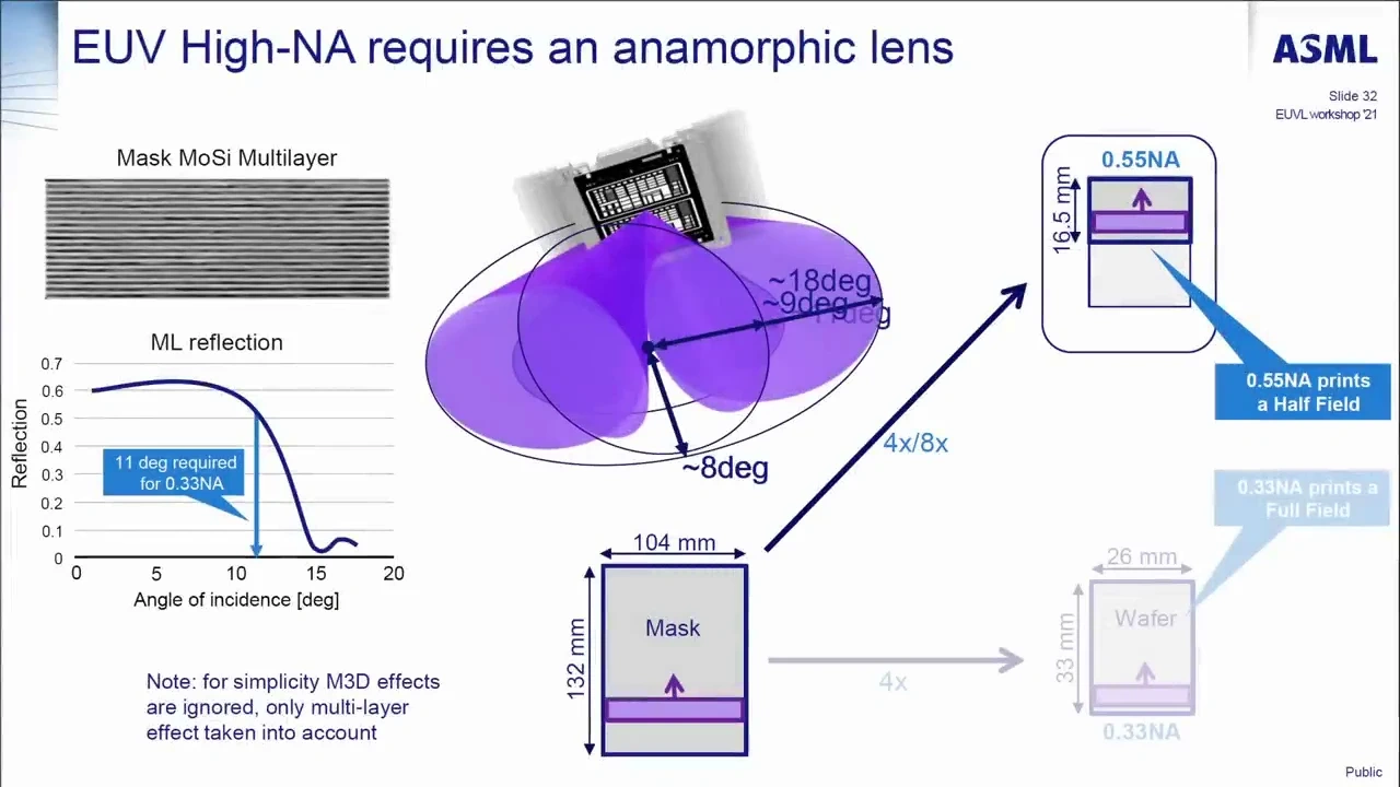
Source: ASML
High NA EUV Rollout Roadmap: A Long-Term Driver
Morgan Stanley further divides the rollout of High NA EUV into three phases, clearly outlining its long path from R&D to mass production:
- Phase One: Initial Introduction
- Timeframe: 2023 to 2026.
- Characteristics: High NA EUV systems (including EXE:5000 and EXE:5200) are primarily delivered to early R&D and pilot customers, such as Intel, Samsung, SK Hynix, TSMC, etc.
- Focus: The core of this phase is for customers to learn how to integrate High NA technology, involving complex process development, mask infrastructure build-out, resist performance optimization, and design enablement. System shipments are limited, primarily for process exploration rather than wafer mass production. SK Hynix's current installation falls within this phase.
- Phase Two: Pilot Production
- Timeframe: 2026 to 2028.
- Characteristics: This phase will involve small-scale manufacturing trials, process qualification, yield improvement, and partial risk production runs, aiming to integrate High NA EUV technology into existing production workflows in preparation for future large-scale mass production.
- Phase Three: Volume Production
- Timeframe: 2027+.
- Characteristics: High NA EUV technology will achieve large-scale production deployment at critical layers of advanced nodes and be fully integrated into production lines.
- Early Adopters: Intel and SK Hynix are expected to be among the first to achieve High NA EUV volume production.
- Later Adopters: Samsung and TSMC are anticipated to implement volume production in the late 2020s or later. For instance, Samsung reportedly installed an EXE:5000 system in March 2025 and plans to use High NA EUV tools for DRAM production targeting its 4F² DRAM architecture in the late 2020s.
Conclusion: The Overture to Long-Term Technological Evolution
In summary, SK Hynix's pioneering introduction of the High NA EUV system is undoubtedly a significant strategic move in advanced memory technology, demonstrating its technological ambition and R&D investment in the era of AI Memory. However, from the perspective of the broader semiconductor industry, this is more of a crucial testing and validation phase before the widespread commercial application of High NA EUV technology. The high equipment costs, complex process integration, and cautious volume production timelines from industry giants all indicate that High NA EUV will be a long-term sales driver for ASML, rather than a technology poised for explosive short-term growth. For the DRAM sector, Morgan Stanley anticipates that High NA EUV volume production will only be realized around 2027, implying that the industry still faces a long path of technological breakthroughs and market maturation before widespread adoption of High NA EUV.


